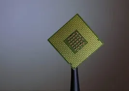
With the rapid development of the semiconductor industry and the continuous emergence of new types of chips, the demand for efficient and accurate testing is also increasing. The semiconductor process flow is complex. According to the "Tenfold Rule" in electronic system fault detection, if chip faults are not detected in time, ten times the cost will be required to troubleshoot and deal with the faults in the next stage. Therefore, the application of semiconductor testing runs through the entire semiconductor manufacturing process and plays a key role in cost control and quality assurance in the semiconductor industry chain.
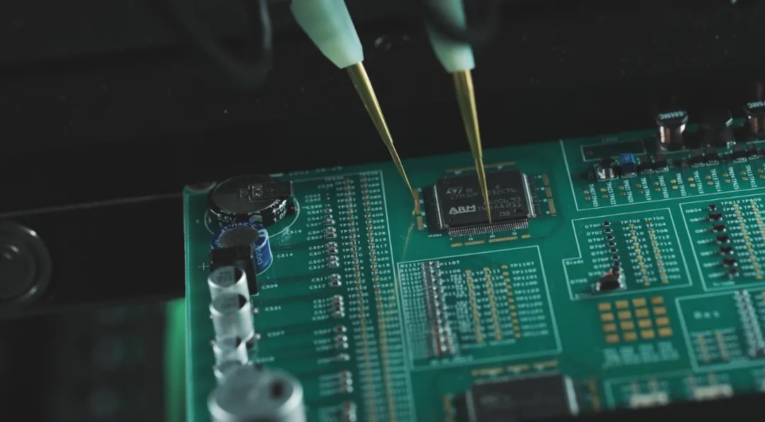
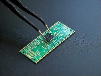
Flying probe testing is a common semiconductor testing technology, which is applicable to various stages of semiconductor chip manufacturing, packaging, and design verification. It can be used to test chips of various models, whether they are discrete devices, integrated circuits, or system-on-chips. Compared with other semiconductor testing methods, flying probe testing can achieve accurate detection of connections between pins, detect the reliability of pin contacts and the quality of signal transmission, eliminate unqualified chips, and ensure product quality. Moreover, flying probes can also perform tests on packaged chips to ensure the reliability of packaging welding connections, which is crucial for guaranteeing the performance of packaged chips.
Application of Flying Probe Testing
01. Testing of Pin Connections and Signal Transmission during Chip Manufacturing:
Flying probe testing technology can detect the connections between pins and the quality of signal transmission during the chip manufacturing process. Through accurate testing, unqualified chips can be eliminated to ensure product quality.
02. Testing of Welding Connections after Chip Packaging:
Flying probe testing technology can test welding connections after chip packaging to ensure the reliability of chips in the working environment.
Flying probe testing technology can conduct pin electrical characteristic tests during the chip design verification stage to ensure the accuracy and reliability of chip design.
Flying probe testing technology can perform quality control and screening in the chip production process to ensure that the quality and performance of products meet requirements.
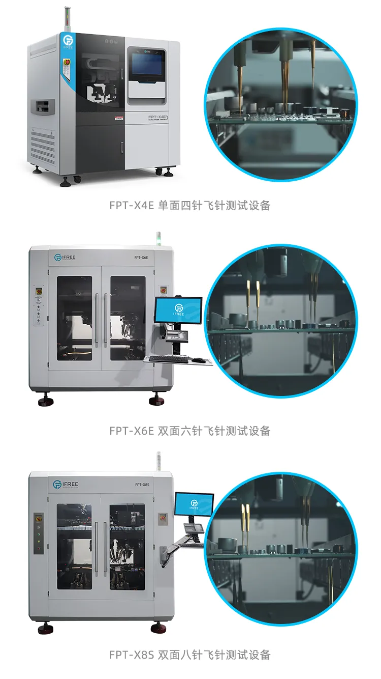
IFREE Flying Probe Testing Equipment
IFREE manufactures multifunctional flying probe testing equipment in China, which features high precision and high speed. The company currently has single-sided four-needle flying probe equipment, double-sided six-needle flying probe equipment, and double-sided eight-needle flying probe equipment, which can be widely used in various application scenarios such as 5G communication, servers, laptops, automotive electronics, medical electronics, aerospace, etc., and provides testing and solutions in them.
Application Examples
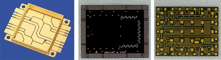
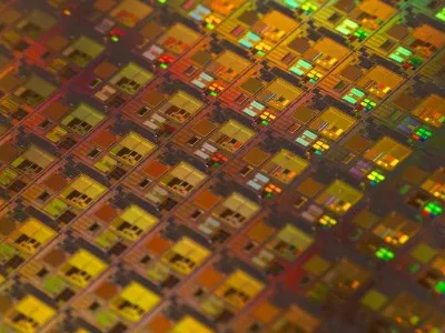
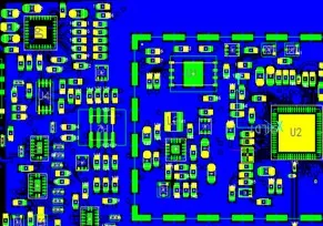
IFREE multifunctional testing solution based on flying probes has been successfully applied in the production and testing process of semiconductor components (such as wafers, bare dies, silicon substrates, ceramic substrates, etc.).
The following takes a bare die of a certain customer as an example to show the application of the IFREE flying probe solution, and the indicators of its product are as follows:
Measurement Point Spacing: 0.2mm
Test Parameters: It is required to test the resistance, capacitance, and inductance values of solder joints on the bare die.
Number of Bare Dies per Strip: 4788 unit/strip
Other Applications