
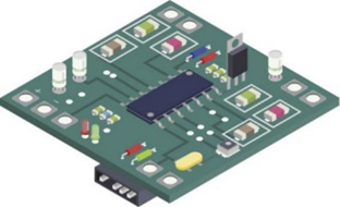
With the popularization of electronic products, the demand for circuit boards in the repair process is also increasing. Traditional circuit board repair methods rely on manual experience and professional knowledge, which are inefficient and prone to errors. Therefore, it is particularly urgent to develop a fully automatic and intelligent circuit board schematic reverse solution redrawing and reverse engineering system.
In order to meet the needs of the industry and customers, based on its independently developed flying probe platform, IFREE has customized and developed a brand new "Intelligent Circuit Board Reverse Engineering System Based on Flying Probe Platform" for users. This system takes full advantage of the fast, accurate, and flexible features of the flying probe platform to achieve rapid testing of circuit boards of different types and sizes, and at the same time provides accurate and reliable test data for users to analyze and judge. The system mainly includes flying probe testing modules, image processing modules, optical recognition modules, data processing modules, etc.
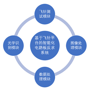
1. Flying Probe Testing Module: The flying probe is a high-precision testing tool, and the measuring module equipped with it can accurately measure the performance indicators of components on the circuit board and the on-off status of circuits.
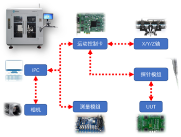
2. Image Processing Module: Through image processing of the flying probe test results, information about the position and size of components on the circuit board can be obtained.
4. Data Processing Module: Through data processing of the recognition results, the reverse solution redrawing and reverse engineering results of the circuit board can be obtained.
This system can well solve the pain points of the traditional circuit board reverse solution redrawing process in terms of efficiency and accuracy, increasing its accuracy by 50% and its efficiency by more than 60%. The system can be divided into two reverse engineering methods. One is non-destructive reverse engineering, which can identify the solder joints of circuit board components and test the circuit board components without damaging the tested board. This method is suitable for the good-bad board comparison test of repair boards. The other is destructive reverse engineering, which needs to be carried out on the premise of removing the components on the circuit board and can more accurately identify the netlist and single component test values. This method is used for the surveying and mapping of detailed files of the tested board.
The following takes non-destructive reverse engineering as an example to illustrate the entire implementation process:
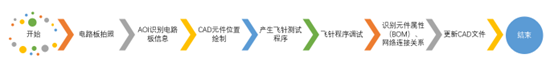
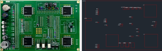
1. Circuit Board Photography: Use a high-resolution camera to take pictures of the entire circuit board to capture detailed information of components and circuits on the circuit board.
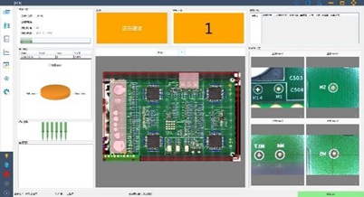
2. AOI Recognition of Circuit Board Information: Use Automatic Optical Inspection (AOI) technology to analyze circuit board photos and identify and extract information such as solder joints, components, coordinates, pins, and silk screen printing on the circuit board.
4. Generation of Flying Probe Test Programs: Generate flying probe test programs using software tools on the flying probe testing instrument according to the EDA component position map. These test programs will be used to control the flying probe testing instrument to test each component and pin on the circuit board.
5. Flying Probe Program Debugging: Load the generated flying probe test programs into the flying probe testing instrument and debug and verify them. Through debugging, it can be ensured that the test programs can correctly access each pin on the circuit board and obtain accurate test results.
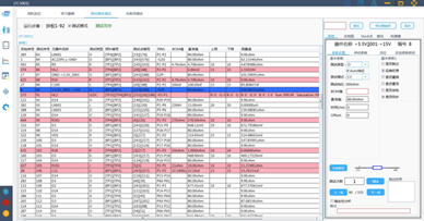
6. Identification of Component Attributes (BOM, Netlist Information): According to the flying probe test programs and test results, identify and determine the attributes of components, including component models, specifications, and electrical characteristics. This information will assist subsequent circuit analysis and component replacement work.
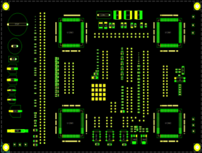
7. Update of EDA Files: Update the EDA component position map and circuit diagrams based on the component attributes and network connection information obtained during the flying probe test. This will assist subsequent circuit analysis and repair work and provide more accurate reference information for maintenance personnel.
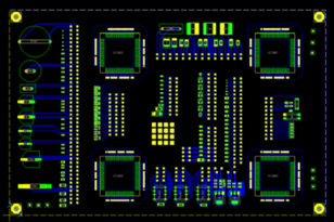
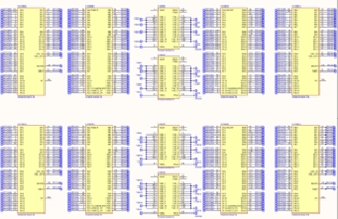
This system uses AOI technology to recognize circuit board information and combines with EDA software to draw component positions and network connection diagrams. Then, flying probe test programs are generated based on the EDA diagrams and are debugged and verified. Through the flying probe test programs, the attributes of components can be identified, and this information is updated into the EDA files to provide more accurate reference information. This process can efficiently obtain accurate information of the circuit board and provide important support for subsequent circuit analysis and repair work.
The "Intelligent Automatic Circuit Board Reverse Engineering System Based on Flying Probes" provided by IFREE is an efficient and accurate intelligent fault diagnosis and circuit reverse engineering tool. It can obtain various information on the circuit board through flying probe testing and perform fault diagnosis, repair plan formulation, etc. based on this information. This system is of great significance in improving repair and reverse engineering efficiency, reducing costs, and reducing risks. In addition, the system developed based on flying probes has the advantages of flexibility, speed, and accuracy. It can perform fault diagnosis during the circuit board production process while meeting repair and reverse engineering needs, greatly enriching the application scenarios of the equipment. This system has been successfully used by multiple users in the industry and has received good feedback and praise.